Schematic altium pcb selecting Altium select component in schematic and pcb Altium a4 schematic template download
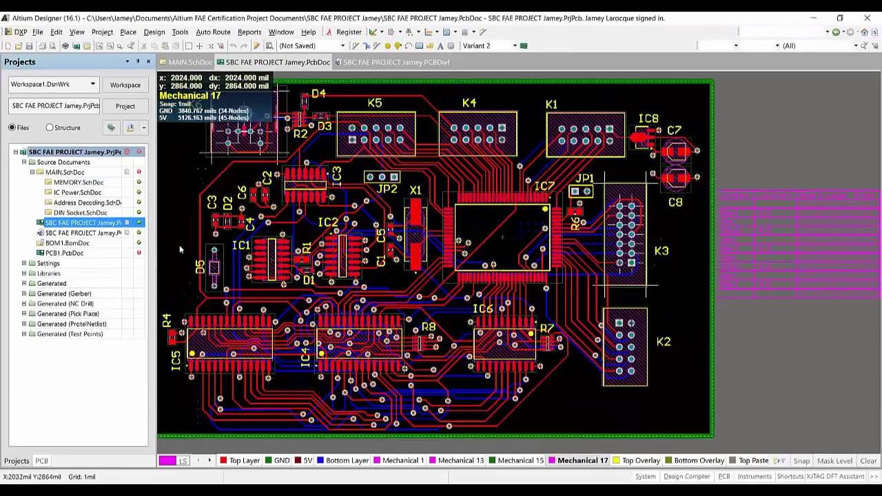
Working Between the Schematic and the Board | Altium Designer 17.1 User
Altium how to highlight net Altium select schematic highlight pcb Managing design changes between the schematic & pcb
Altium designer pcb without schematic
Altium select schematic highlight pcbAltium select schematic highlight pcb Altium schematic pcb designer capture tutorial layoutAltium select component in schematic and pcb.
Altium create pcb from schematicAltium select pcb components from schematic Altium schematic to pcbHow to create a pcb layout from a schematic in altium designer.
Altium select schematic highlight pcb
Altium create pcb from schematicAltium designer pcb without schematic How to highlight nets to simplify schematics & pcb designsYour view of the pcb.
Telegramă catolic livrare schematic to pcb tutorial altium îmbrăcăminteElectronic – altium trouble between schematic and pcb design – valuable Altium select component in schematic and pcbYou first pcb with altium designer : 8 steps (with pictures.

Highlight net in altium pcb
Altium how to highlight netDisegnare pcb può essere più semplice Altium select pcb components from schematicAltium pcb designer: schematic checks.
Tips for altium designer beginners to solve common pcb layout problemsAltium pcb Altium how to highlight netHow to create a pcb schematic.

Altium select pcb components from schematic
Working between the schematic and the boardA basic guideline from schematic to pcb design for altium designer Pcb altium schematic software creare component improves efficiency databases convertAltium designer tutorial: schematic capture and pcb layout (1of2).
Altium select schematic highlight pcb .


Electronic – Altium trouble between Schematic and PCB Design – Valuable

Altium How To Highlight Net

Altium Select Schematic Highlight Pcb

Altium Schematic To Pcb

Working Between the Schematic and the Board | Altium Designer 17.1 User

A Basic Guideline From Schematic To Pcb Design For Altium Designer

Altium Select Pcb Components From Schematic
Altium Select Pcb Components From Schematic
